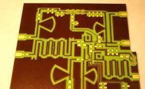
Component Placement in RF PCB Design
RF PCBs contain a variety of components that work together to achieve the desired functionality. The different parts, including the antenna, amplifiers, filters, and the power supply, are positioned to minimize interference and signal loss. This is done by optimizing the placement of each component to minimize parasitic capacitance and inductance, as well as to avoid electromagnetic coupling between circuits. RF PCBs also often include shielding to protect the internal components from external electromagnetic radiation.
One of the biggest challenges in RF circuits is skin effect, which occurs when alternating currents flow on the surface of a conductor, increasing its resistance and causing it to inadvertently couple with adjacent conductors. In RF PCBs, this can cause cross-talk between signals, which reduces signal performance and can lead to interference and data corruption. Another issue is coupling between closely spaced components and traces, which can also reduce signal performance. RF circuits are especially susceptible to these issues because of their high frequencies.
To minimize these issues, RF PCB designers use different techniques to improve the design process. These include using a low aspect ratio for via holes and keeping them free of gaps or discontinuities. They also make sure that the traces that are crossing multiple layers are as short as possible to minimize parasitic inductance. Finally, they use decoupling capacitors to ensure that the signal paths are clean.
The Role of Component Placement in RF PCB Design
In addition, rf pcb require careful consideration of the material choice for each layer and component to ensure that they have the right thermal expansion properties. For example, the dielectric constant of the PCB material, as well as the thickness and copper foil size, must match the requirements for each RF signal path. The copper foil must also have a low water absorption rate, as it can affect the electrical performance of the circuit board.
Other key considerations for RF PCBs include proper grounding and signal routing, which are important for improving circuit performance. For instance, a common mistake is to route an RF trace and a normal signal track parallel to each other, which can lead to signal interference. Instead, a more effective solution is to place them at a 45° angle from each other. This not only increases the surface area of the circuit board, but also allows for more direct routing of RF signals, minimizing their length and reducing attenuation.
The final element of a successful RF circuit is the layout, which includes the arrangement and order of the conductive and dielectric layers in the circuit board. Typically, the RF signal layer is on the top layer, while the ground and power planes follow it. The RF signal layer should be as close to the ground plane as possible, which will help minimize electromagnetic interference between the two layers.