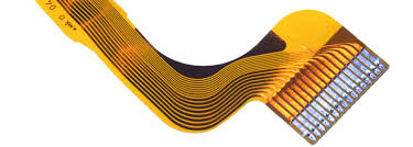
Radius For Flexible PCB Boards
The maximum bending radius for flexible PCB boards depends on the materials and construction used. Pushing flex materials beyond their recommended capabilities can lead to failures that take time and money to fix. Fortunately, a good understanding of the limitations and capabilities of the materials and construction can help engineers determine what the best bending radius is for their design.
In general, the higher the number of layers in a flex board, the larger the minimum bending radius needed to avoid stress and damage. This is due to the fact that additional layers introduce more rigidity and make it harder for the board to bend without causing mechanical problems. However, there are some exceptions to this rule. For example, some flex circuits are made using a bonded construction, which increases the strength of the layers and allows for a smaller minimum bending radius.
To increase the bending radius of a flexible pcb board, designers can use special copper features and materials. For instance, the use of a fully annealed copper (FACT) core is helpful because it provides better ductility. This makes it easier for the circuit board to withstand mechanical stress during assembly and rework.
Maximum Bending Radius For Flexible PCB Boards
It is also important to minimize the number of components located close to folding areas of the flex circuit. This will prevent stress from concentrating on these areas during bending and help protect the circuit from damage. In addition, the use of annular rings can help reduce stress concentration spots by spreading the load over a wider area.
Trace routing is another key factor in the bending tolerance of a flex circuit. It is best to route traces perpendicular to the bending axis, and to use wider traces in bending zones to distribute stress over a greater area. The use of alignment features like notches, registration marks or holes can also help ensure accurate folding and positioning during assembly. Finally, incorporating fold-state simulations into the PCB design process can allow designers to verify that the bending radius chosen for their design is sufficient to avoid stress-related failures and defects.
The maximum bending radius for a flex PCB board is determined by the amount of pressure that the copper can bear without suffering damage or failure. It is important to identify this radius early in the design phase to ensure that the PCB can be bent properly without causing damage to the copper or other structural defects.
To maximize the bending radius of a flex circuit, it is important to use a high-quality FACT laminate with a low thermal coefficient and a wide temperature range. In addition, it is best to use a high-quality, roll-annealed copper. This copper has a better ductility than sputtered or hard rolled copper, making it ideal for flex PCBs. Lastly, it is best to avoid using plated through-holes or components in a flex zone to protect the circuit from excessive stress during bending and assembly. This will also minimize the chances of pad peeling and trace lifting.